2026-11-04 · Fonte:TechPowerUp
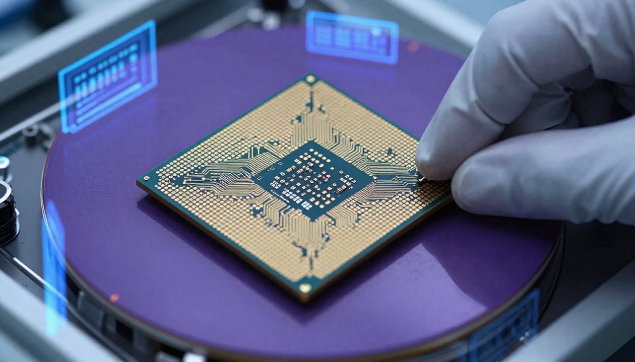
An 80% yield on the 114.304 mm² compute tile signals low defects and strong parametric performance for Intel Foundry's 18A node, with Nova Lake reportedly set to follow.
Intel's "Panther Lake" system-on-chip, whose compute tile is manufactured on the company's in-house 18A process node, has reportedly reached an 80% yield, according to a new report. The figure amounts to a notable vote of confidence for Intel Foundry, whose 18A yields have been climbing steadily.
The compute die at the heart of the chip measures approximately 8.004 by 14.288 millimeters, for a total silicon area of 114.304 mm². Hitting roughly 80% yield on that footprint points to more than just low defect rates on the node — it also indicates a high parametric yield, meaning a significant number of dies emerge with all functioning elements intact. Taken together, the figures suggest Intel is overcoming its historically stubborn parametric yield problems alongside its manufacturing challenges.
That progress may already be reshaping Intel's next-generation plans. In a shift recently rumored, the company intends to produce the majority of "Nova Lake" compute tiles internally, with roughly 80-90% of output manufactured by Intel Foundry and the remainder placed with TSMC. The arrangement amounts to a deliberate dual-sourcing strategy, but the heavy weighting toward Intel's own fabs underscores rising confidence in the 18A line.
On defect metrics, a node as mature as 18A would typically be expected to post defect rates near D0=0.1 or D0=0.2. Given the advancements baked into the process and months of high-volume production with "Panther Lake," Intel has likely reached the lower end of that span. Combined with the relatively small compute tile used in this SoC, the resulting parametric yields look strong — evidence that the node's trajectory is firmly on the right track.
Tags: Intel · Panther Lake · Intel Foundry · Intel 18A · Nova Lake · Chip Yields
萬安算交所 AIXX · AIXX · Exchange verificado · Ir ao mercado